Research
Research overview
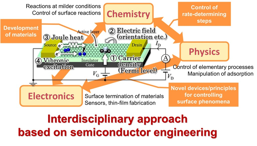
Various interfaces are inherently present in electronic devices. In the case of a field-effect transistor, which is a representative electronic device, charge carriers (such as electrons) are injected from the electrode (source) through the electrode/semiconductor interface, and the injected carriers propagate near the semiconductor/insulator interface and eventually flow out to the opposite electrode (drain). Therefore, understanding and successfully controlling these interfaces can improve the performance of electronic devices and impart new functionality. From the opposite point of view, it is also possible to investigate the interface phenomena themselves by studying the device characteristics. In our laboratory, we are conducting research aimed at understanding the properties of interfaces through device configurations and providing new functions to devices by controlling the interfaces.
Recently, two-dimensional (2D) materials with atomically thin bodies have become available. A typical example is graphene, which is obtained by peeling off only one monatomic layer of graphite. Owing to their ultimate thinness, 2D materials are strongly susceptible to surface phenomena such as molecular adsorption. Our laboratory aims to establish a new fundamental scientific methodology, "field-effect surface science," in which device structures are used as tools to control surface phenomena.